Thermal oxide or silicon dioxide layer is formed on bare silicon surface at temperature range from 900°C ~ 1200°C . Compared to CVD deposited oxide layer, thermal oxide has a higher uniformity, and higher dielectric strength. In most silicon- based devices, thermal oxide layer play an important role to pacify the silicon surface , to act as doping barriers and as surface dielectrics . Celsa provides quality and standard thermal oxide wafer in diameter from 2” to 6” . If you need special layer thickness please contact us.
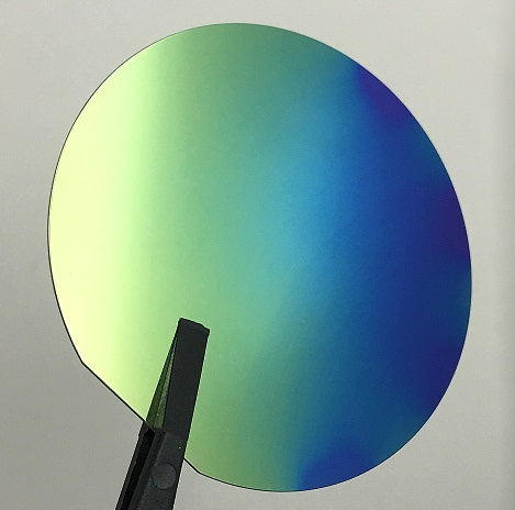
Thermal oxide Layer
SiO2 layer on Silicon wafer Oxide layer thickness: Check the variations for silica thickness Refractive index - 1.455
Silicon Wafer Specifications: Check the variations for Wafer size, Silica thickness, Conductive Type, Polish, and Resistivity (If you would like to measure the resistivity accurately, please order our Portable 4 Probe Resistivity Testing Instrument.) Surface roughness, Ra: < 5A (RMS)